Last Updated: 5th March 2021
NESRGB
Installation Guide
Famicom
Table of Contents
Tools and materials required
- Soldering iron and leaded solder wire
- Insulated copper ‘hook up’ wire. It’s better to use wire that is thin and easy to work with.
- Solder sucker or desoldering iron to remove the PPU.
- Pliers and cutters
- Round file
- Drill with a step drill bit which goes up to 8mm (optional)
Check contents and prepare
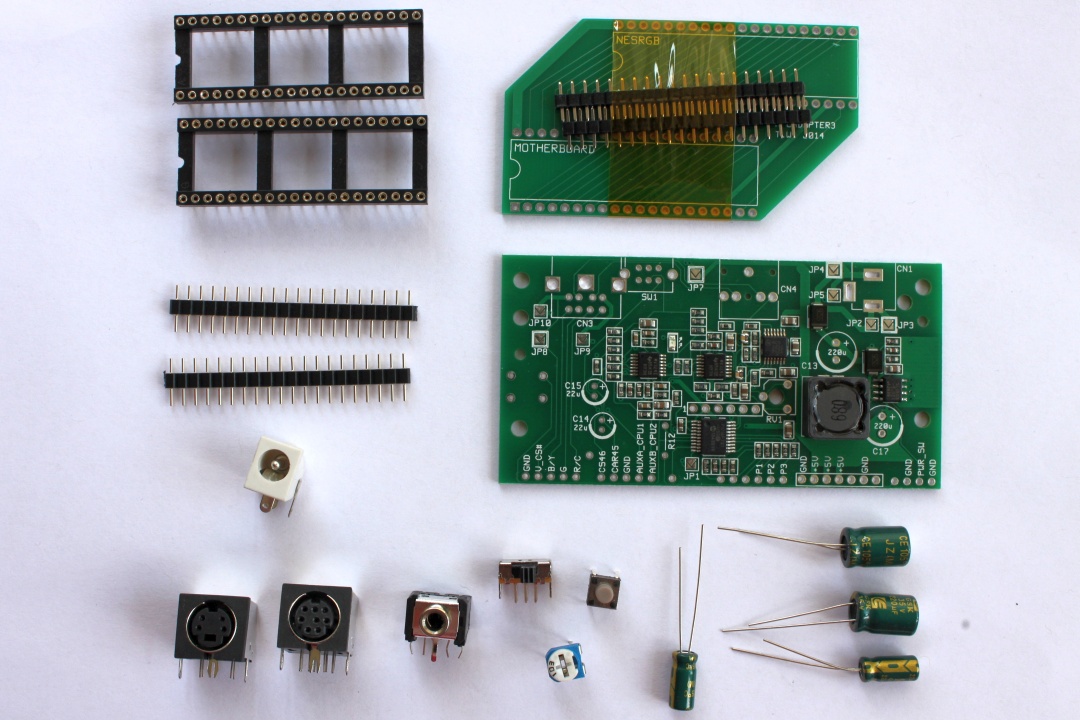
The following parts are included with the kit for the Famicom (original).
- 2 * 40 pin DIP round pin IC sockets
- 2 * 20 pin round pin strip
- 1 * 2.1mm DC barrel socket
- 1 * s-video 4 pin mini-DIN socket
- 1 * 8 pin mini-DIN socket
- 1 * audio 3.5mm jack socket
- 1 * two-position slide switch
- 1 * 10k trimmer potentiometer
- 1 * tactile push switch
2 * 22u electrolytic capacitor(no longer required in v1.1)- 2 * 220u electrolytic capacitor
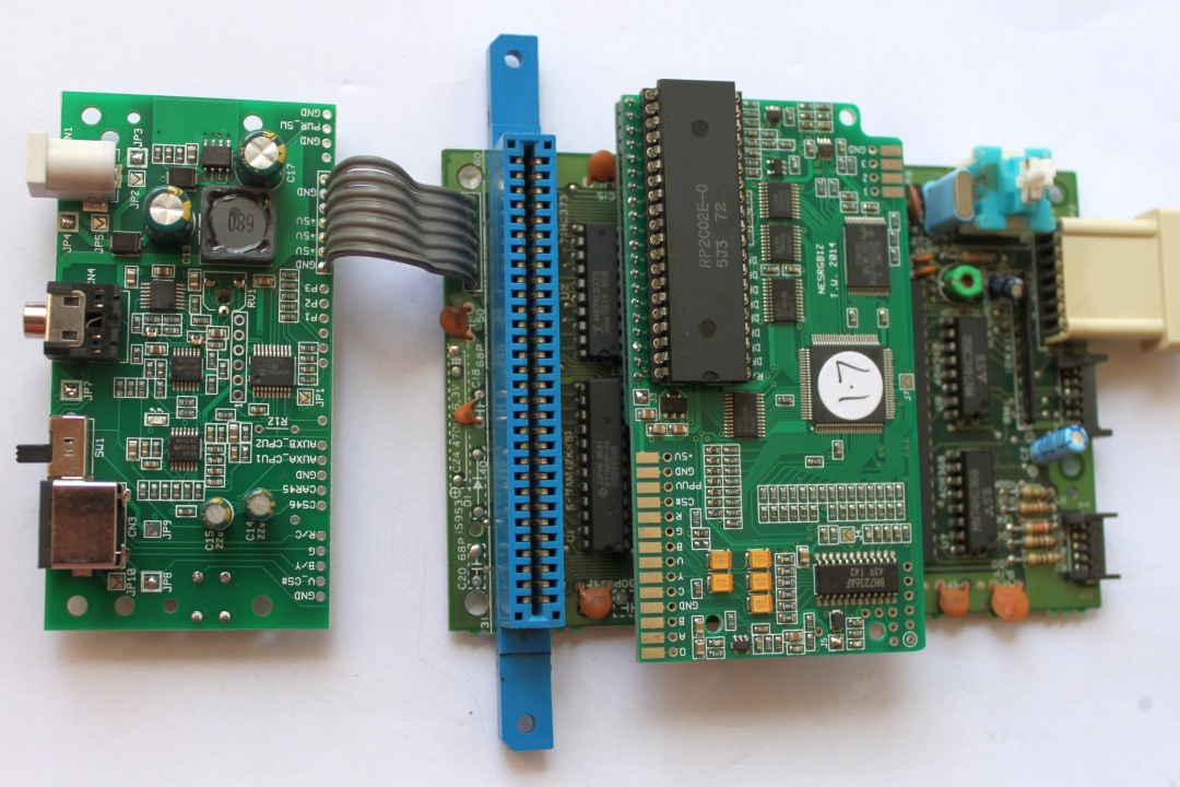
- adapter board #3 for Famicom (original)
- 2 * 20 pin square pin strip (taped to adapter board)
- Famicom Power/Audio board
- NESRGB board (not pictured)
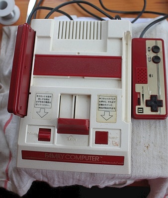
Open the Famicom by removing the six Philips head screws from the bottom.
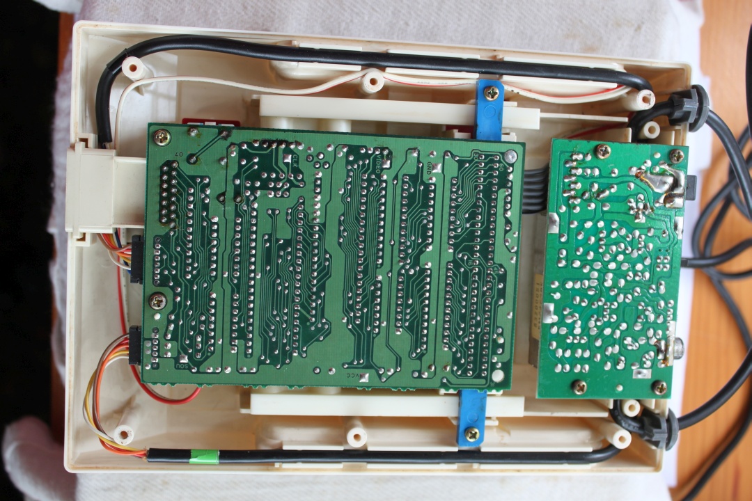
This is the older version Famicom with a completely separate board for the power regulator and RF modulator.
This is the newer version Famicom which has a large metal shield holding the motherboard and the power/RF board together.
This guide will focus on the older version but contain specific information about the newer version where necessary.
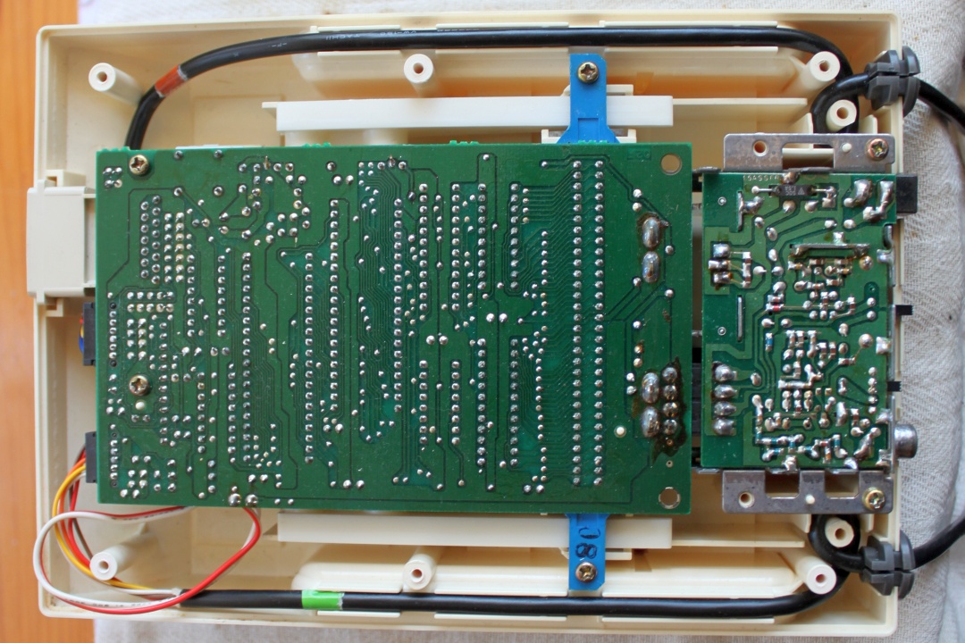
Remove the screws holding down both boards. Use the solder sucker to desolder the power switch wires and 7 pin ribbon cable to the power/RF board. The power/RF board is no longer required and may be disposed of.
The newer version Famicom has four large metal tabs which must be desoldered before the power/RF board can be removed.
The cartridge eject mechanism must be removed to fit the NESRGB board.
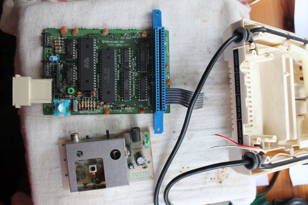
Mount the NESRGB board
Identify and desolder the PPU. This can be tricky because the motherboard’s holes are plated through. Please read the article here: Desoldering the PPU.
Run the hot soldering iron against each pin of the PPU chip to remove solder burrs.
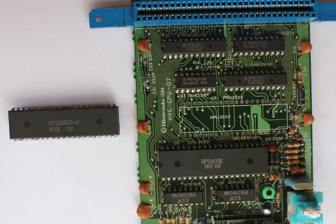
Install one of the 40p round pin IC sockets in place of the PPU.
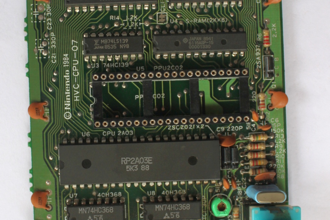
Insert the two round pin strips into the socket.
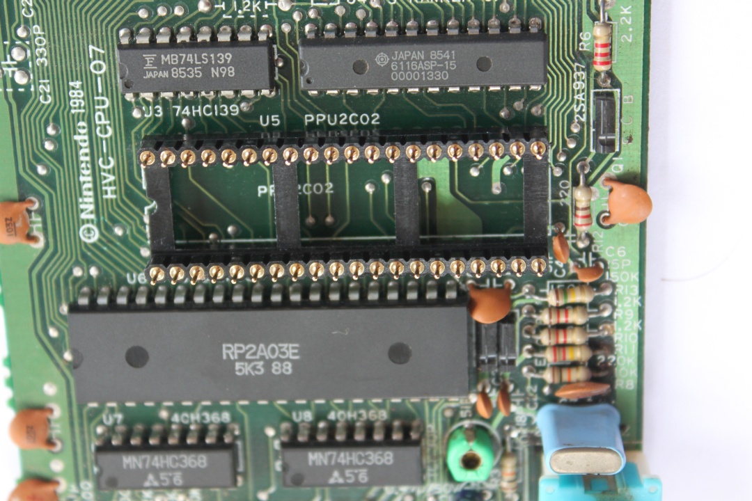
Place the adapter board over the pins in the place labelled MOTHERBOARD.
With a finger on the adapter board, solder the adapter board pins in place. This way, the pins will be straight and aligned correctly.
Carefully remove the adapter board from the motherboard.
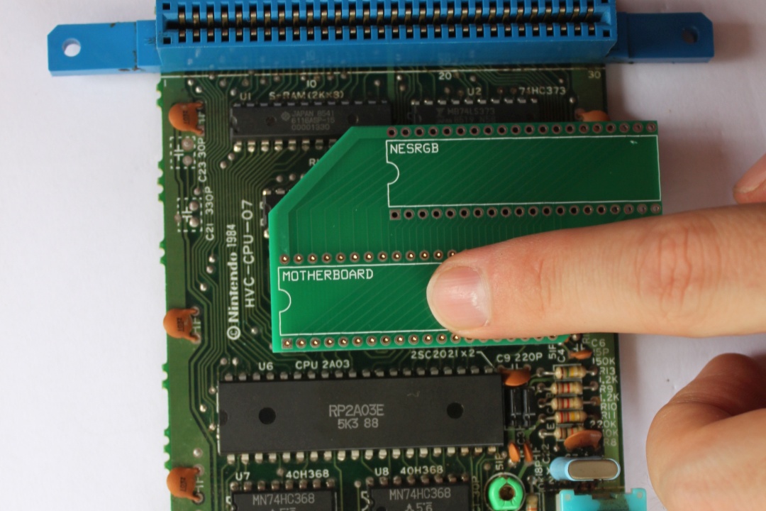
Take the NESRGB board out of its packaging.
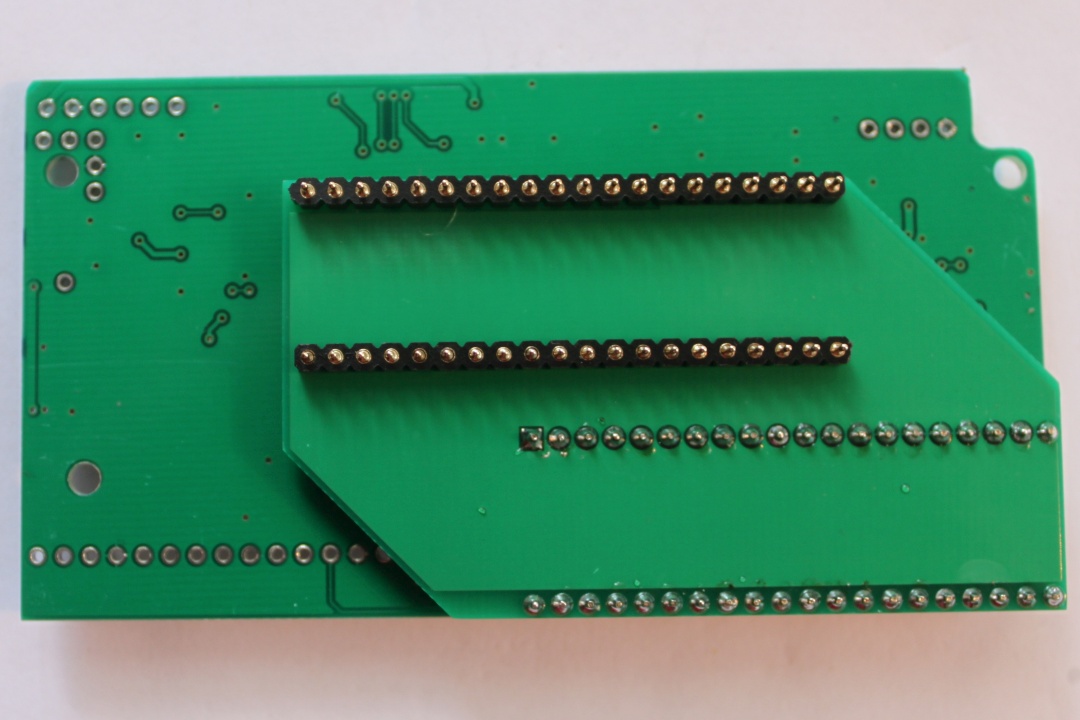
Insert two square pin strips into the underside of the NESRGB board. Place the adapter board over the pins like so.
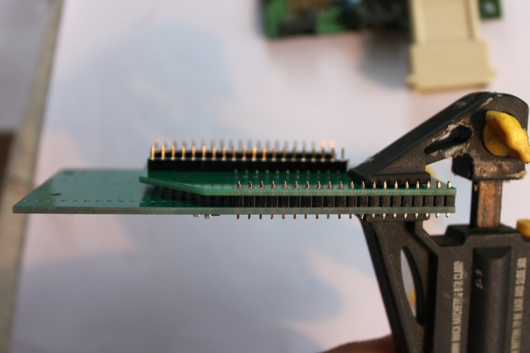
Hold two boards together against the edge of the table and solder one side of the square pins into the NESRGB board. This way, the pins will be straight and aligned correctly.
Remove the adapter board.
Solder the second 40p round pin IC socket in place on the NESRGB board.
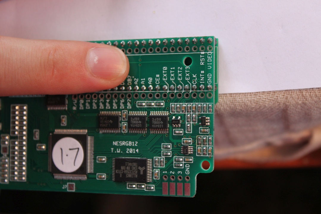
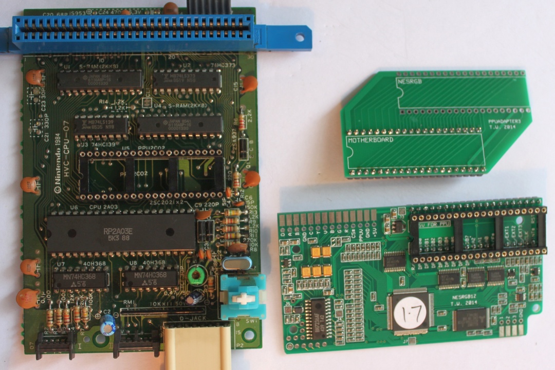
Now check you have done everything correctly so far.
You should have:
- A Famicom motherboard with the PPU removed and 40p round pin IC socket soldered in its place.
- An adapter board with round pin soldered in the MOTHERBOARD position
- A NESRGB board with square pins soldered underneath and a 40p round pin IC socket soldered on top in the correct position.
Solder the NESRGB board to the adapter board.
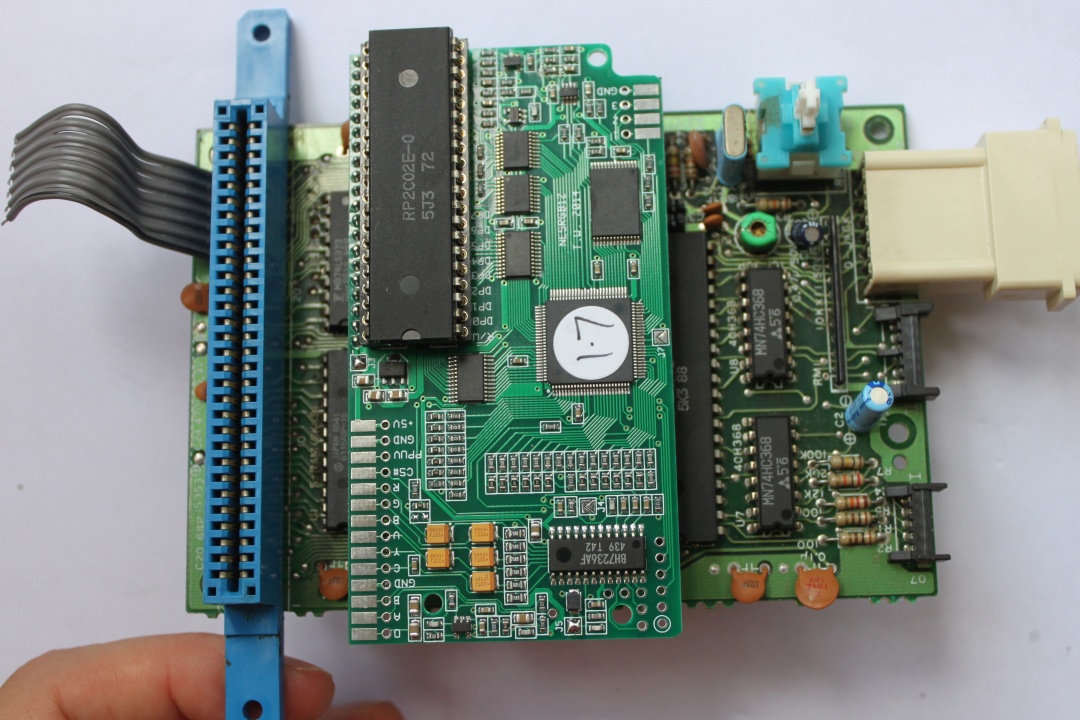
Pop the PPU into the socket on the NESRGB board and insert the finished NESRGB assembly into the Famicom motherboard socket. Solder jumpers J3 (for power) and J5 (NTSC video).
Put aside.
Assemble and configure the New Power/Audio board
The Power/Audio board looks like this. It comes partially assembled. It requires some connectors and other parts attached before it can be installed.
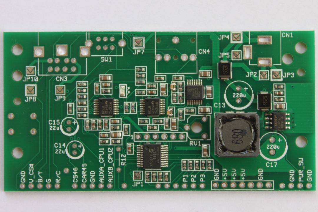
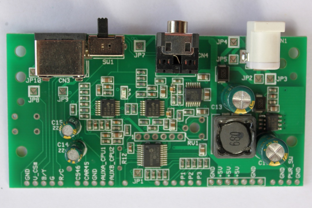
CN3 – The video output connector. Fit either the 4p S-VIDEO mini-DIN connector or the 8p RGB mini-DIN. Solder the jumpers according to the table below.
| JP7 | JP8 | JP9 | JP10 | |
| S-VIDEO 4p | OPEN | OPEN | CLOSED | CLOSED |
| RGB 8p | CLOSED | CLOSED | OPEN | OPEN |
SW1 – The Everdrive audio compensation switch. There is a popular flash cartridge called the Everdrive N8. This device can emulate audio chips found inside some cartridges. The problem is the audio output level is lower from an Everdrive than a normal cartridge. When the switch is in the CH2 position the cartridge audio mixing level is boosted to compensate. Set to the CH1 position for all other cartridges.
CN4 – The audio output connector, a 3.5mm jack socket. This is a switch jack. This means the audio signal will be output from this connector when a cable is plugged into it. If there is nothing plugged in, the audio signal is switched to the 8p mini-DIN RGB connector. This jack must be used for audio if the s-video 4p mini-DIN is fitted.
CN1 – Power input, 2.1mm barrel socket. The original Famicom power supply may be used, along with other centre negative power supplies like the one for the Sega Master System/Mega Drive. Alternatively, the polarity of the power supply may be changed to suit modern switching power supplies. Solder the jumpers according to the table below.
| JP2 | JP3 | JP4 | JP5 | |
| Centre negative (Famicom, Sega Master, etc.) | OPEN | CLOSED | CLOSED | OPEN |
| Centre positive (modern switching PSU) | CLOSED | OPEN | OPEN | CLOSED |
C14, C15 – Electrolytic capacitors, 22u, required. These components are polarised, make sure they go in the right way.
C13, C17 – Electrolytic capacitors, 220u, required. These components are polarised, make sure they go in the right way.
JP1 – This jumper controls the operation of the LED near the middle of the board. When the jumper is open, the LED is normally on and visible as a dim red light shining through the air grille at the Famicom’s rear. The light blinks off whenever the palette is changed. If the jumper is closed, the state of the light is reversed. It is normally off and blinks on only when the palette is changed.
Solder in the components. Make sure they are all sitting flat against the board.
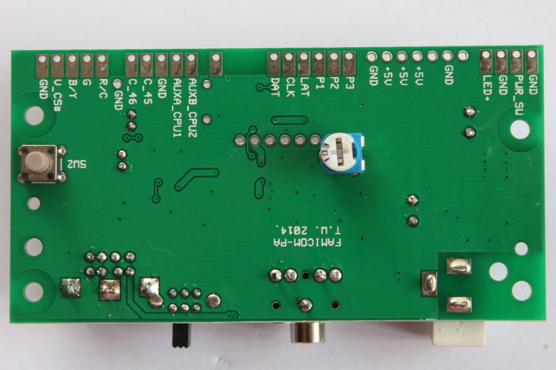
There are two methods to change the colour palette. The first is to push SW2 (if installed). The second is to hold down a particular combination of buttons on the P1 control pad. The combination is START+SELECT+RIGHT in that order. You can tap right to cycle through the three palettes.
The optional palette button, SW2, may be mounted on the top (with all the other components), the board’s underside or can be omitted entirely. The benefit to mounting on the underside is that the adjustment may be accessed through a hole in the shell’s bottom after the unit is assembled.
Most people will probably want to omit SW2 because it is practical to change the palette via the P1 control pad combination method. In this guide, it will be fitted to the bottom of the board.
The stereo audio width adjustment controls the amount of separation between the two square channels (CPU1) and the noise/triangle channel (CPU2). It may be set between no separation and total separation. Like the palette button, this adjustment may be fitted to either the board’s top or bottom. It may not be omitted.
If no stereo separation is desired, RV1 should be mounted on the board’s topside and rotated fully anticlockwise.
Solder some wires
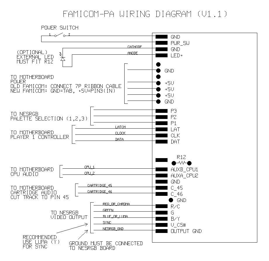
The CPU audio labels have been corrected on the current P/A board version (v1.1).
Cut away some plastic about 2mm deep out of the interior wall of the top shell. This is required so the PPU will fit.
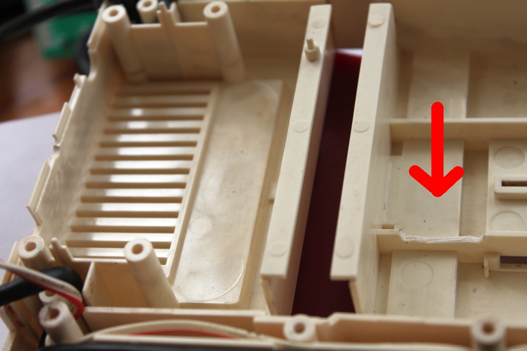
Use the round file to remove some plastic from the TV/GAME opening in the top half of the shell so that the audio output jack will fit through.
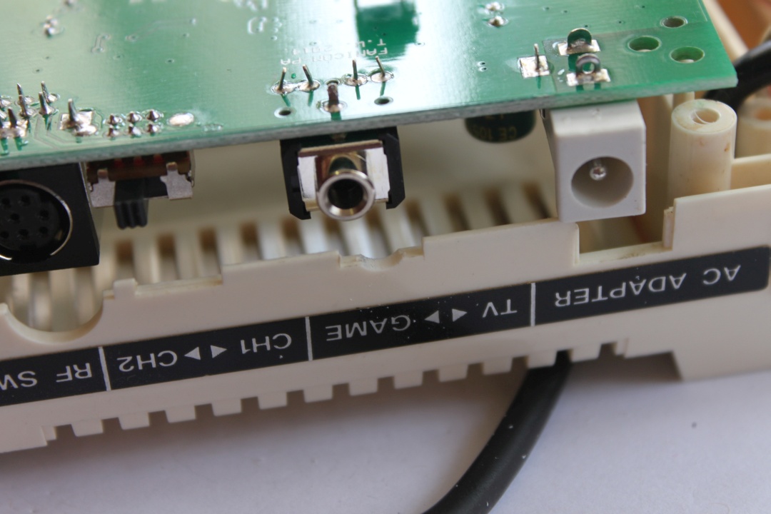
Old version Famicom pins and power supply connection:
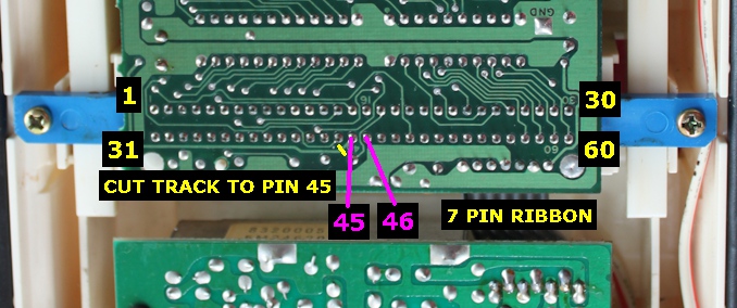
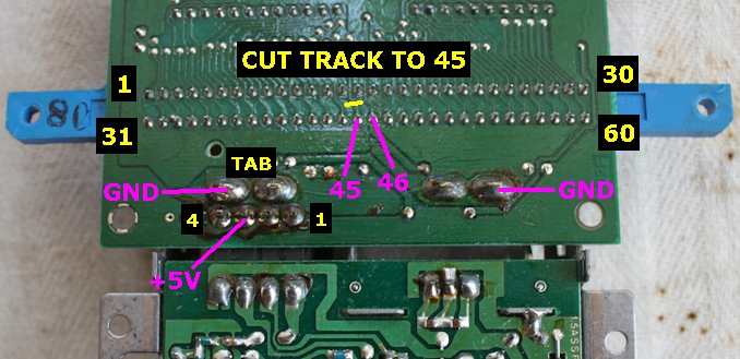
New version Famicom pins and power supply connection:
For the old version Famicom, Solder the 7 wire ribbon cable to the P/A board.
For the new version solder wires between the GND and +5V points on the P/A board and motherboard as indicated by the diagram above. Use thicker wires here. Two wires +5V, two wires for Ground for lower resistance.
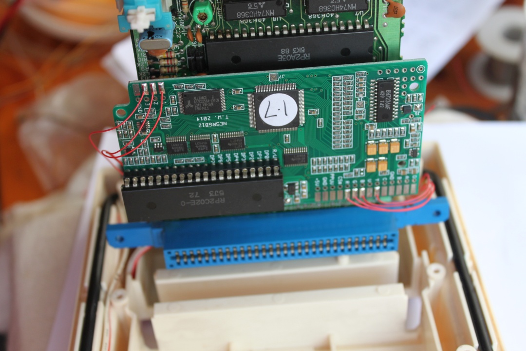
Solder wires to the palette selection pads labelled 1, 2, 3.
Solder wire to the video pads. If you have installed the S-Video 4p connector on the P/A board, you should connect wires to the Y and C pads. If you have installed the RGB 8p connector, you should connect the wire to the R, G, B, and another for the sync signal (labelled V_CS# on the P/A board). I recommend using the Y signal for sync as it is the most compatible, but V or CS# or PPUV may be used.
There is no need to connect the ground pins as there is already a solid connection to ground through the PPU socket.
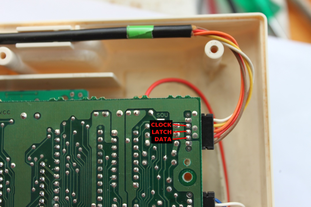
Connect three wires to the pins on the player 1 controller port. They may be wires up to the LAT, DAT, and CLK pins on the P/A board. This will allow the player to swap the palette by pressing START+SELECT+RIGHT (in this order only) on the controller.
The audio signals need to be wired up. These include the two audio signals from the CPU pins 1 and 2—labelled AUXA_CPU1 and AUXB_CPU2.
The previous version of the P/A board (v1.0) had an error on labels for the CPU audio points. Labels for CPU1 and CPU2 were swapped around. They have been corrected on the current version (v1.1).
Audio from CPU pin 1 is connected to AUXB_CPU2.
Audio from CPU pin 2 is connected to AUXA_CPU1.
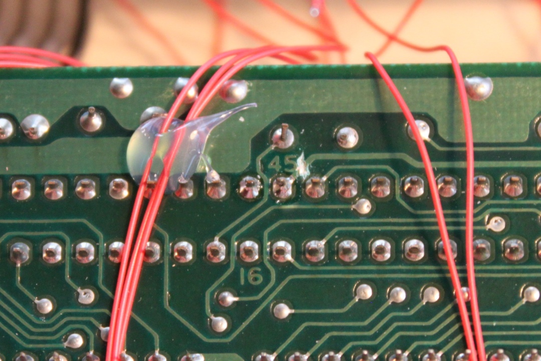
Connect wires between cartridge pins 45, 46, and the pads on the P/A board labelled C_45 and C_46. This is for the cartridge audio mixing. The track to pin 45 must be cut on the Famicom motherboard.
Solder the power switch wires between PWR_SW and GND. The new version Famicom has short wires for the power switch which will have to be replaced with longer ones to reach the P/A board pads.
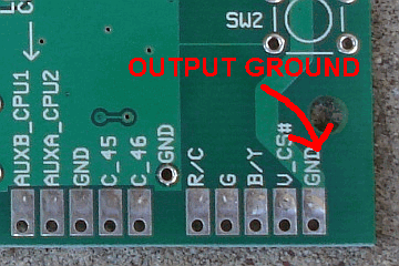
The new version 1.1 of the P/A board has the ground for the output (audio, video) connectors electrically isolated from the ground connection on the rest of the board. This change was made to prevent noise from the power supply from interfering with the video signals.
Correct operation requires a wire between the NESRGB board GND point and the output ground point on the P/A board.
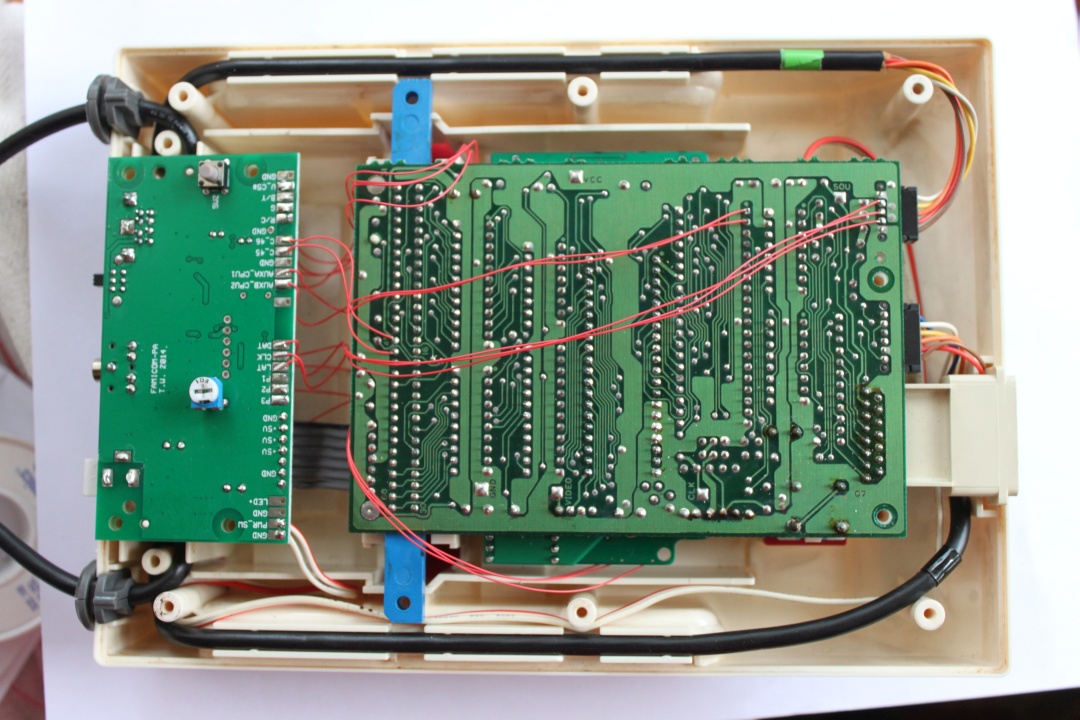
Once everything is wired up, put the screws back in which hold the motherboard and P/A board in place and test to make sure everything is working.
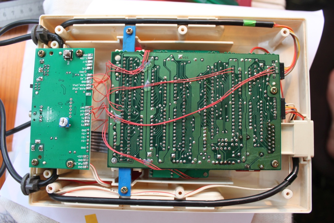
Screw it back together. Done.
Stick the wires in place with some hot glue.
If you have mounted either SW2 and RV1 on the underside of the P/A board you will need to drill a hole (or two) of 8mm diameter in the base for access.
Instead of finding the spot to drill by measuring from the base plastic’s edge, I recommend this method. Start by cutting some squares of electrical tape (or any other tape) and stick them over SW2 and/or RV1.
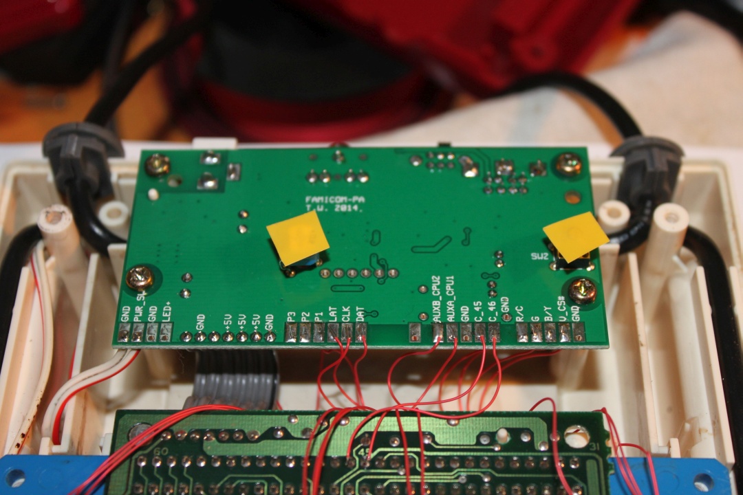
Stick a ball of blue tack (or your local equivalent of a poster hanging putty) on each piece of tape.
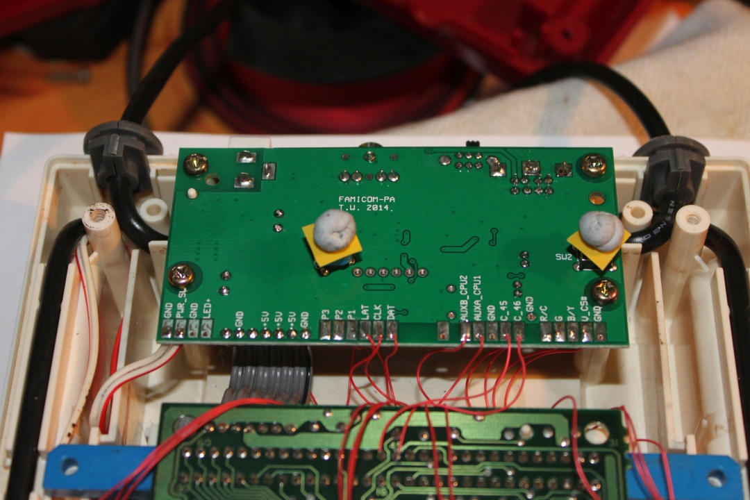
Close the two halves of the shell and press together firmly. Pull them apart again, and the blue tack is now stuck to the base plastic showing an imprint of the component.
Mark the centre with something pointy. Drill an 8mm hole at each location with a step drill bit,
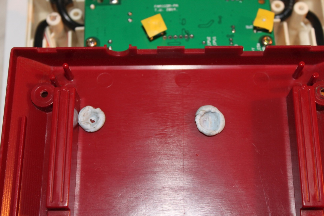
Close the two halves of the together again and put the six Philips screws back in.
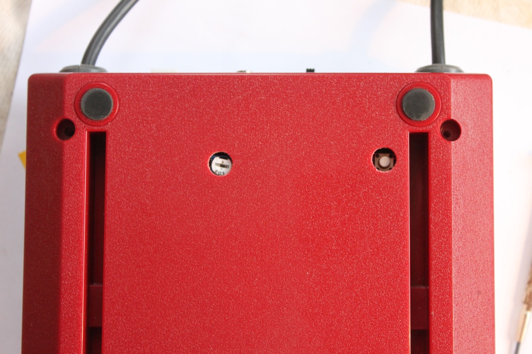
The rear of the console now looks like this.
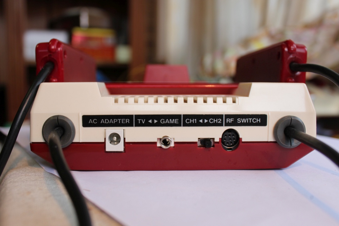
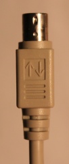
Due to the way it’s mounted, the video connector is recessed into the console by the shell’s thickness at the rear. This presents a problem is if the cable to match has a short nose. It cannot be inserted far enough into the socket to make contact with the pins.
The solution is simple. Use a sharp knife to cut away some of the moulded plastic around the plug on the cable.

