
Last Updated: 5th March 2021
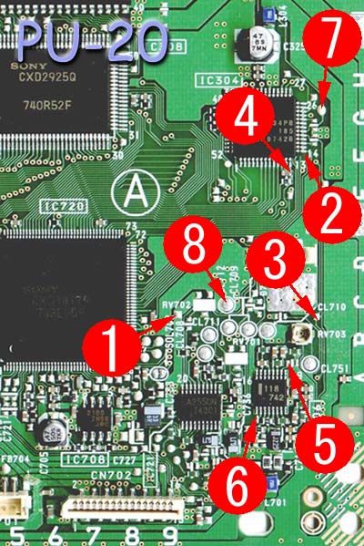
Mayumi V4 PU 20 Diagram
Notes
The diagram isn’t the cleanest so I’d like to clarify a few points that are unclear.
Pin six connects to the bottom left most leg of that chip, and pin five connects to the pad to the left of the white line on the board.
Pin four connects to the right side of the capacitor, which is the topmost component in that spot.
The second pin connects to the bottom leg of the right side of that chip. Be careful not to use too much solder or you might connect two legs of the chip together.
Installation Tips
- Cut your wires to be as short as possible
- The high speed clock line (pin 2) needs to be especially short and carefully routed.
- Placing the chip where pin eights circle is seems to be the ideal location.
- Be careful when soldering to pin four if you apply too much solder, or press too hard, you may knock a component off the board, or bridge the connection with nearby points.
- When soldering to pin six be careful, you don’t want to apply too much solder and bridge nearby pins on the chip.